Research

Soft semiconductor materials development
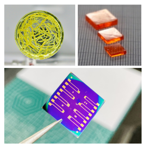
‘Soft Semiconductors’, SoS, may well present a class of optoelectronic materials that can be quite distinct from standard inorganic semiconductors (e.g., Si, GaAs, CdTe). The reason is that in a SoS some of the constituents are held by weak van der Waals forces or loose ionic bonds. The SoS class includes molecular crystals, halide perovskites, conjugated polymers, small organic molecule-based solids, van der Waals heterostructures and quantum dot films. Especially striking is the low density of optoelectronic active defects for the, mostly inorganic, Pb halide perovskite compounds, because these, as many other SoS, can be prepared at low temperatures. We aim to find out which chemistries and/or physical properties in soft semiconductors that is responsible for their low defect densities, to guide design of new materials with these properties and develop new class electronic materials. We grow single crystals and thin-films of the materials and investigate the opto-electronic properties using various spectroscopic and electronic measurements.

Electronic doping of soft semiconductor

In pristine organic or perovskite materials, the number of charge carriers is less which is responsible for the low conductivity. The dopants introduce extra charge carriers (i.e, more numbers of free electrons or holes) which increases its conductivity. Though some very basic understanding is available regarding the electronic doping of organic and perovskite materials, the doping process is not fully understood. There is a need to provides design rules for more efficient dopant processes/ materials for which a more detailed understanding of the doping process is needed. We develop new doping methods and dopants for low-cost semiconductors like organic or halide perovskite materials to further improve the efficiency of devices based on this material

Photophysics and Spectroscopy
The photophysics of organic semiconductors and perovskites explores how these materials interact with light, influencing their electronic and optical properties. In organic semiconductors, photoexcitation generates excitons (electron-hole pairs), which can diffuse through the material before recombining. This exciton diffusion plays a crucial role in charge transport and device performance. Perovskite materials, on the other hand, exhibit strong light absorption and efficient charge carrier generation due to their unique crystal structure. The photophysics of perovskites involves understanding processes such as charge separation, recombination, and migration, which directly impact their photovoltaic and optoelectronic applications. Both fields are actively researched for their potential in various technological applications like solar cells, LEDs, and photodetectors.
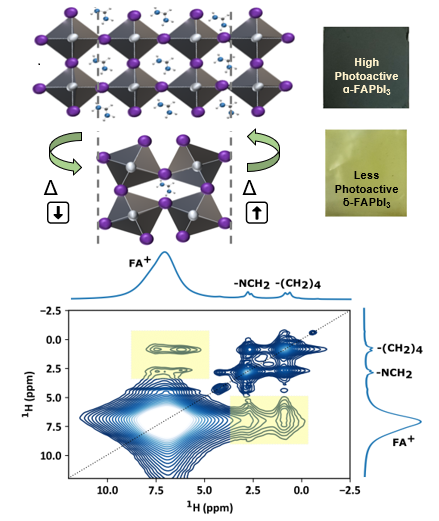
Additionally, we employ a range of spectroscopic techniques, including UV-Vis, PL, IR, solution, and solid-state spectroscopy, to gain molecular-level insights into the structure-property relationship.
Mesoscopic Optoelectronic devices
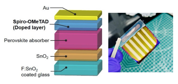
We utilize newly developed SoS materials, along with doping techniques, in the fabrication of various electronic devices such as solar cells, light-emitting diodes (LEDs), and transistors. By integrating these materials into device applications, we aim to extract pertinent data crucial for enhancing our fundamental comprehension and advancing optoelectronic technologies. These materials offer unique properties like tunable band gap and high carrier mobility, making them promising candidates for next-generation electronic devices. Through systematic experimentation and analysis, we strive to unravel the underlying mechanisms governing their behaviour within these devices, driving innovation and progress in the field of optoelectronics.

